The Nanophotonics Technology Center (NTC, www.ntc.upv.es) is a research institute at UPV. NTC is a leader in Europe in knowledge generation, development and integration of innovative photonic technologies and systems. Its mission is to generate new knowledge in micro- and nanofabrication of structures on silicon and silicon-related photonic technologies for the development of nanotechnology and nanoscience, mainly towards their application in areas such as telecom networks and systems, biophotonics, defence, security, photonic computation, or photovoltaics. NTC has been involved in several European projects in FP5, FP6, FP7 and H2020, acting as coordinator in many of them, as well as in projects for the European Space Agency or the European Defence Agency. NTC is forming part of the European alliance for photonic manufacturing ePIXFab (http://www.epixfab.eu/).
- Design and simulation of plasmonic, photonic and phononic structures at the nanoscale: numerical tools such as COMSOL, Rsoft FullWave/FimmProp and CST Microwave Studio are available.
- Micro and nanofabrication: 500 sqm clean room (class 10-100) for 6” Si wafer processing. Available processes are: lithography (two e-beam direct writers, coater, developer, mask aligner and DUV line stepper), dielectric, metal and polySi deposition, thickness measurement, sputtering, etch and chemical cleans, ICP-RIE, rapid-thermal annealing, ion implantation and full lab for physical characterization (Raman spectrometry, SEM, FTIR spectrometer, AFM and ellipsometer). Such processes have been successfully used in the past to fabricate: i) plasmonic nanostructures (Au, Ag, Al) on silicon and glass substrates using electron beam lithography + lift-off with resolution ~20 nm; ii) planar optical metamaterials with activity in the near infrared; iii) optomechanical crystals in silicon with cavities showing state-of-the-art Q-factors for mechanical and optical modes; iv) metallic nanostructures on silicon and silicon nitride suspended membranes for generation of GHz acoustic phonons; v) plasmonic bow-tie nanoantennas integrated in silicon nitride waveguides for single-antenna SERS.
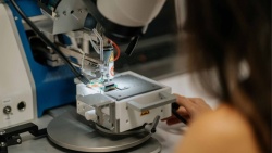
- Optical characterization laboratory: Five set-ups for characterization of photonic integrated chips are available, including advanced 5-axis stations for optical characterisation and performance test allow end-fire as well as grating-coupler-enabled measurements of transmission and reflection with high dynamic range (>60 dB). A tapered-fiber loop set-up for characterization of GHz optomechanical cavities is working since Jan 2017. Optical oscilloscope with 65 GHz electrical bandwidth and picosecond pulsed lasers for pump-probe experiments in the NIR are also available.
- THz lab: Terahertz time domain spectroscopy (THz-TDS) up to 2.5 THz. Characterization of microwave photonics systems (amplitude and phase) up to 110 GHz. Si bolometer for THz measurements in the FTIR spectrometer (spanning from 0.5 to 400 THz).


